- 您现在的位置:买卖IC网 > Sheet目录1998 > ICS843251BGI-15LF (IDT, Integrated Device Technology Inc)IC CLK GEN ETHERNET 25MHZ 8TSSOP
ICS843251I-15
FEMTOCLOCKCRYSTAL-TO-3.3V, 2.5V LVPECL CLOCK GENERATOR
IDT / ICS 3.3V, 2.5V LVPECL CLOCK GENERATOR
3
ICS843S51BGI-15 REV. A NOVEMBER 2, 2012
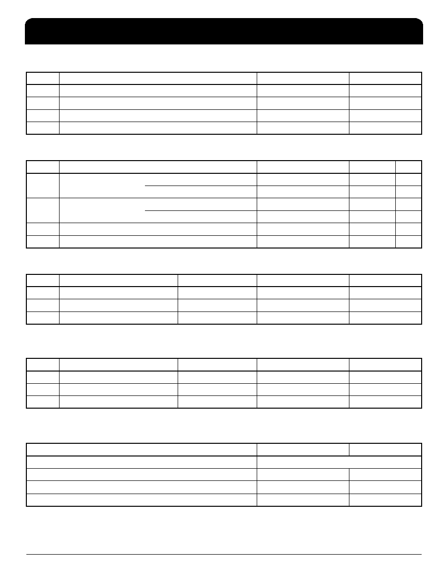
Table 3B. Power Supply DC Characteristics, VCC = 2.5V ± 5%, VEE = 0V, TA = -40°C to 85°C
Table 3C. LVCMOS/LVTTL DC Characteristics, VCC = 3.3V ± 5% or 2.5V ± 5%, VEE = 0V, TA = -40°C to 85°C
Table 3D. LVPECL DC Characteristics, VCC = 3.3V ± 5%, VEE = 0V, TA = -40°C to 85°C
NOTE 1: Outputs termination with 50
to V
CC – 2V.
Table 3E. LVPECL DC Characteristics, VCC = 2.5V ± 5%, VEE = 0V, TA = -40°C to 85°C
NOTE 1: Outputs termination with 50
to V
CC – 2V.
Table 4. Crystal Characteristics
NOTE: It is not recommended to overdrive the crystal input with an external clock.
Symbol
Parameter
Test Conditions
Minimum
Typical
Maximum
Units
VCC
Core Supply Voltage
2.375
2.5
2.625
V
VCCA
Analog Supply Voltage
VCC – 0.08
2.5
VCC
V
IEE
Power Supply Current
78
mA
ICCA
Analog Supply Current
8mA
Symbol
Parameter
Test Conditions
Minimum
Typical
Maximum
Units
VIH
Input High Voltage
VCC = 3.3V
2
VCC + 0.3
V
VCC = 2.5V
1.7
VCC + 0.3
V
VIL
Input Low Voltage
VCC = 3.3V
-0.3
0.8
V
VCC = 2.5V
-0.3
0.7
V
IIH
Input High Current
VCC = VIN = 3.465V or 2.625V
150
A
IIL
Input Low Current
VCC = 3.465V or 2.625V, VIN = 0V
-5
A
Symbol
Parameter
Test Conditions
Minimum
Typical
Maximum
Units
VOH
Output High Current; NOTE 1
VCC – 1.4
VCC – 0.9
A
VOL
Output Low Current; NOTE 1
VCC – 2.0
VCC – 1.7
A
VSWING
Peak-to-Peak Output Voltage Swing
0.6
1.0
V
Symbol
Parameter
Test Conditions
Minimum
Typical
Maximum
Units
VOH
Output High Current; NOTE 1
VCC – 1.4
VCC – 0.9
A
VOL
Output Low Current; NOTE 1
VCC – 2.0
VCC – 1.5
A
VSWING
Peak-to-Peak Output Voltage Swing
0.4
1.0
V
Parameter
Test Conditions
Minimum
Typical
Maximum
Units
Mode of Oscillation
Fundamental
Frequency
23.2
30
MHz
Equivalent Series Resistance (ESR)
40
Shunt Capacitance
7pF
发布紧急采购,3分钟左右您将得到回复。
相关PDF资料
ICS843253AGI-45LF
IC SYNTHESIZER LVPECL 16-TSSOP
ICS8432DY-101LFT
IC SYNTHESIZER 700MHZ 32-LQFP
ICS8432DYI-101LF
IC SYNTHESIZER 700MHZ 32-LQFP
ICS843SDNAGLF
IC GENERATOR FEMTOCLOCK 8TSSOP
ICS844001AGLFT
IC CLK GEN FIBRE CHAN 8-TSSOP
ICS844002AG-01LF
IC SYNTHESIZER 2LVDS 20-TSSOP
ICS844002AGI-01LFT
IC SYNTHESIZER 2LVDS 20-TSSOP
ICS844002AGLF
IC SYNTHESIZER 2LVDS 20-TSSOP
相关代理商/技术参数
ICS843251BGI-15LFT
功能描述:IC CLK GEN ETHERNET 25MHZ 8TSSOP RoHS:是 类别:集成电路 (IC) >> 时钟/计时 - 时钟发生器,PLL,频率合成器 系列:HiPerClockS™, FemtoClock™ 标准包装:1,000 系列:- 类型:时钟/频率合成器,扇出分配 PLL:- 输入:- 输出:- 电路数:- 比率 - 输入:输出:- 差分 - 输入:输出:- 频率 - 最大:- 除法器/乘法器:- 电源电压:- 工作温度:- 安装类型:表面贴装 封装/外壳:56-VFQFN 裸露焊盘 供应商设备封装:56-VFQFP-EP(8x8) 包装:带卷 (TR) 其它名称:844S012AKI-01LFT
ICS843251BGI-15T
制造商:Integrated Device Technology Inc 功能描述:IC SYNTHESIZER LVPECL 8TSSOP
ICS843251I-12
制造商:ICS 制造商全称:ICS 功能描述:FEMTOCLOCKS? CRYSTAL-TO-3.3V, 2.5V LVPECL CLOCK GENERATOR
ICS8432-51K
制造商:ICS 制造商全称:ICS 功能描述:700MHZ, CRYSTAL-TO-3.3V DIFFERENTIAL LVPECL FREQUENCY SYNTHESIZER
ICS843252
制造商:ICS 制造商全称:ICS 功能描述:FEMTOCLOCKS⑩ CRYSTAL-TO-3.3V LVPECL FREQUENCY SYNTHESIZER
ICS843252-04
制造商:ICS 制造商全称:ICS 功能描述:FEMTOCLOCKS⑩ CRYSTAL-TO-3.3V LVPECL CLOCK GENERATOR
ICS843252AG
制造商:ICS 制造商全称:ICS 功能描述:FEMTOCLOCKS⑩ CRYSTAL-TO-3.3V LVPECL FREQUENCY SYNTHESIZER
ICS843252AG-04
制造商:ICS 制造商全称:ICS 功能描述:FEMTOCLOCKS? CRYSTAL-TO-3.3V LVPECL CLOCK GENERATOR